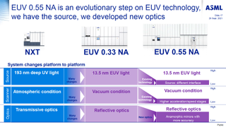
Samsung is set to start installing its first EUV lithography tool with a 0.55 numerical aperture (High-NA) in Q4 2024 – Q1 2025, reports Seoul Economic Daily, citing its sources. The device will be used primarily for research and development purposes as the company works on its next-generation process technologies that require resolutions enabled by High-NA EUV tools. Samsung also works on a High-NA ecosystem with Lasertec, JSR, Tokyo Electron, and Synopsys.
Samsung's first ASML Twinscan EXE:5000 High-NA lithography system will be installed at the company's Hwaseong campus, where it will develop its next-generation fabrication technologies for logic and DRAM. The unit is projected to be operational by mid-2025. As a result, Samsung will have its first High-NA EUV tool operational about a year later than Intel, but it will still be ahead of its rivals TSMC and SK hynix. When Samsung adopts High-NA EUV for mass production, it remains to be seen, but it is not expected unti l well into the decade's second half.
Samsung plans to develop a robust ecosystem around high-NA EUV technology. In addition to acquiring the high-NA EUV litho equipment, Samsung is collaborating with Japan's Lasertec to develop inspection equipment specifically for high-NA photomasks. According to DigiTimes, Samsung has reportedly purchased Lasertec's high-NA EUV mask inspection tool, the Actis A300.
"Using [High-NA EUV-specific tool] to inspect semiconductor masks has improved the contrast ratio by over 30% compared to conventional [EUV-specific tool]," said Dr. Min Cheol-ki from Samsung Electronics' Semiconductor Research Institute at the 2024 Lithography + Patterning Symposium.

According to DigiTimes, Samsung is also collaborating with JSR, a maker of photoresists, and Tokyo Electron, a maker of etching machines, to prepare for commercial implementation of High-NA EUV tools by 2027. Samsung is also working with Synopsys to shift from traditional circuit designs to curvilinear patterns on photomasks. This change is expected to improve the precision of circuits imprinted on wafers, which is critical for furt her refinements of process technologies.
ASML's High-NA EUV Twinscan EXE tool is set to achieve an 8nm resolution, substantially improving the current Low-NA EUV systems that max out at 13nm with a single exposure. This advancement will make transistors about 1.7 times smaller, nearly three times the transistor density. While Low-NA systems can also reach this level of resolution and density, they require the costly and complex double patterning process. The shift to High-NA EUV technology is expected to eliminate the need for double patterning, simplify production, potentially improve yields, and reduce costs.
Achieving these 8nm critical dimensions is crucial for producing chips with sub-3nm process technologies. Yet, at 2nm-class nodes, virtually all chipmakers will be using double patterning. Intel is also adopting pattern-shaping tools for its 20A node. The American chip giant only plans to use High-NA EUV with its 14A node.
Meanwhile, the leap to high-NA brings its own set of challenges. High-NA EUV tools are more expensive ($380 million—$400 million) and have a halved imaging field, which will require significant changes in chip design. Additionally, the larger size of high-NA EUV systems compared to low-NA systems means chipmakers will need to rethink their fab layouts to accommodate these new machines.

0 Comments
Post a Comment